- 您现在的位置:买卖IC网 > Sheet目录2006 > LTC2498IUHF#TRPBF (Linear Technology)IC ADC 24BIT 16CH 38-QFN
LTC2498
18
2498ff
applications inForMation
INPUT DATA FORMAT
The LTC2498 serial input word is 13 bits long and contains
two distinct sets of data. The first set (SGL, ODD, A2, A1,
A0) is used to select the input channel. The second set of
data(IM,FA,FB,SPD)isusedtoselectthefrequencyrejec-
tion,speedmode(1x,2x),andtemperaturemeasurement.
After power-up, the device initiates an internal reset cycle
whichsetstheinputchanneltoCH0–CH1(IN+=CH0,IN–=
CH1),thefrequencyrejectiontosimultaneous50Hz/60Hz,
and 1x output rate (auto-calibration enabled). The first
conversion automatically begins at power-up using this
default configuration. Once the conversion is complete,
a new word may be written into the device.
The first 3 bits shifted into the device consist of two preen-
able bits and one enable bit. As demonstrated in Figure 3,
the first three bits shifted into the device enable the device
configurationandinputchannelselection.Validsettingsfor
these three bits are 000, 100 and 101. Other combinations
should be avoided. If the first three bits are 000 or 100, the
following data is ignored (don’t care) and the previously
selected input channel and configuration remain valid for
the next conversion.
If the first 3 bits shifted into the device are 101, then the
next 5 bits select the input channel for the next conversion
cycle, see Table 3.
The first input bit following the 101 sequence (SGL)
determines if the input selection is differential (SGL = 0)
or single-ended (SGL = 1). For SGL = 0, two adjacent
channels can be selected to form a differential input. For
SGL = 1, one of 16 channels is selected as the positive
input.ThenegativeinputisCOMforallsingleendedopera-
tions. The remaining 4 bits (ODD, A2, A1, A0) determine
which channel(s) is/are selected and the polarity (for a
differential input).
The next serial input bit immediately following the input
channel selection is the enable bit for the conversion
configuration (EN2). If this bit is set to 0, then the next
conversion is performed using the previously selected
converter configuration. This is useful in systems using
the same rejection/speed for all input channels and for
backwardcompatibilitywiththeLTC2418/LTC2414families
of delta sigma ADCs.
A new configuration can be loaded into the device by
setting EN2 = 1, see Table 4. The first bit (IM) is used
to select the internal temperature sensor. If IM = 1, the
following conversion will be performed on the internal
temperaturesensorratherthantheselectedinputchannel.
The next 2 bits (FA and FB) are used to set the rejection
frequency. The final bit (SPD) is used to select either the
1x output rate if SPD = 0 (auto-calibration is enabled and
the offset is continuously calibrated and removed from
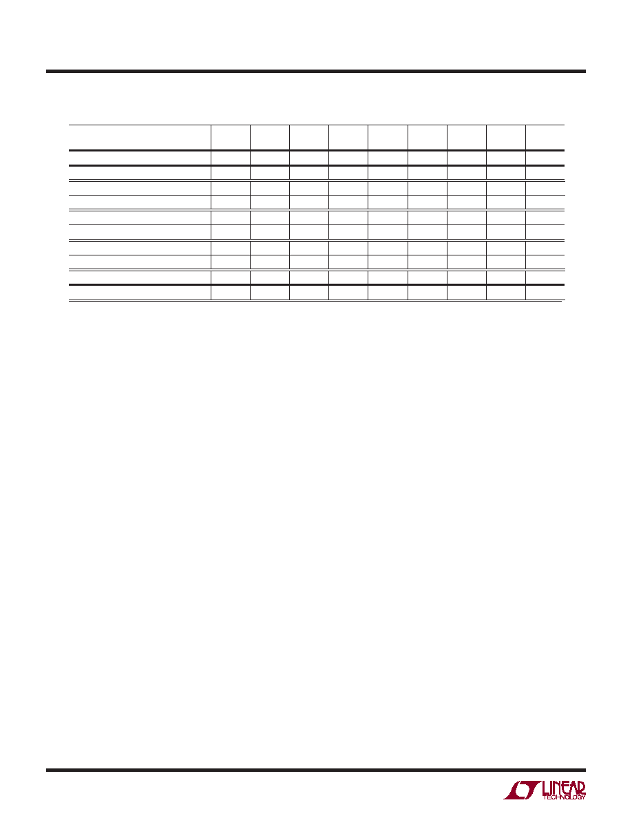
Table 2. Output Data Format
Differential Input Voltage
VIN*
Bit 31
EOC
Bit 30
DMY
Bit 29
SIG
Bit 28
MSB
Bit 27
Bit 26
Bit 25
…
Bit 0
VIN* ≥ 0.5 VREF**
0
1
0
…
0
0.5 VREF** – 1LSB
0
1
0
1
…
1
0.25 VREF**
0
1
0
1
0
…
0
0.25 VREF** – 1LSB
0
1/0***
0
1
…
1
0
1
0
…
0
–1LSB
0
1
…
1
–0.25 VREF**
0
1
0
…
0
–0.25 VREF** – 1LSB
0
1
0
1
…
1
–0.5 VREF**
0
1
0
…
0
VIN* < –0.5 VREF**
0
1
…
1
*The differential input voltage VIN = IN+ – IN–. **The differential reference voltage VREF = REF+ – REF–.
***The sign bit changes state during the 0 output code when the device is operating in the 2x speed mode.
发布紧急采购,3分钟左右您将得到回复。
相关PDF资料
LTC2600IUFD#PBF
IC DAC OCTAL R-R 16BIT 20-QFN
LTC2602IMS8#TRPBF
IC DAC 16BIT DUAL R-R VOUT 8MSOP
LTC2604IGN-1#TRPBF
IC DAC 16BIT QUAD R-R OUT 16SSOP
LTC2605IGN-1#TRPBF
IC DAC 16BIT OCT I2C 16-SSOP
LTC2606IDD#TRPBF
IC DAC 16BIT I2C V-OUT 10-DFN
LTC2607IDE#TRPBF
IC DAC 16BIT R-R I2C 12-DFN
LTC2609CGN#PBF
IC DAC 16BIT R-R QUAD 16SSOP
LTC2621IDD-1#PBF
IC DAC 12BIT R-R 10-DFN
相关代理商/技术参数
LTC2499CUHF
制造商:Linear Technology 功能描述:ADC Single Delta-Sigma 7.5sps 24-bit Serial 38-Pin QFN EP
LTC2499CUHF#PBF
功能描述:IC ADC 24BIT DELTA SIG 38-QFN RoHS:是 类别:集成电路 (IC) >> 数据采集 - 模数转换器 系列:- 标准包装:1 系列:microPOWER™ 位数:8 采样率(每秒):1M 数据接口:串行,SPI? 转换器数目:1 功率耗散(最大):- 电压电源:模拟和数字 工作温度:-40°C ~ 125°C 安装类型:表面贴装 封装/外壳:24-VFQFN 裸露焊盘 供应商设备封装:24-VQFN 裸露焊盘(4x4) 包装:Digi-Reel® 输入数目和类型:8 个单端,单极 产品目录页面:892 (CN2011-ZH PDF) 其它名称:296-25851-6
LTC2499CUHF#TRPBF
功能描述:IC ADC 24BIT DELTA SIG 38-QFN RoHS:是 类别:集成电路 (IC) >> 数据采集 - 模数转换器 系列:- 标准包装:1,000 系列:- 位数:16 采样率(每秒):45k 数据接口:串行 转换器数目:2 功率耗散(最大):315mW 电压电源:模拟和数字 工作温度:0°C ~ 70°C 安装类型:表面贴装 封装/外壳:28-SOIC(0.295",7.50mm 宽) 供应商设备封装:28-SOIC W 包装:带卷 (TR) 输入数目和类型:2 个单端,单极
LTC2499CUHFPBF
制造商:Linear Technology 功能描述:24bit Delta Sigma ADC Temp Sens LTC2499
LTC2499IUHF#PBF
功能描述:IC ADC 24BIT DELTA SIG 38-QFN RoHS:是 类别:集成电路 (IC) >> 数据采集 - 模数转换器 系列:- 标准包装:1 系列:microPOWER™ 位数:8 采样率(每秒):1M 数据接口:串行,SPI? 转换器数目:1 功率耗散(最大):- 电压电源:模拟和数字 工作温度:-40°C ~ 125°C 安装类型:表面贴装 封装/外壳:24-VFQFN 裸露焊盘 供应商设备封装:24-VQFN 裸露焊盘(4x4) 包装:Digi-Reel® 输入数目和类型:8 个单端,单极 产品目录页面:892 (CN2011-ZH PDF) 其它名称:296-25851-6
LTC2499IUHF#TRPBF
功能描述:IC ADC 24BIT DELTA SIG 38-QFN RoHS:是 类别:集成电路 (IC) >> 数据采集 - 模数转换器 系列:- 标准包装:1,000 系列:- 位数:16 采样率(每秒):45k 数据接口:串行 转换器数目:2 功率耗散(最大):315mW 电压电源:模拟和数字 工作温度:0°C ~ 70°C 安装类型:表面贴装 封装/外壳:28-SOIC(0.295",7.50mm 宽) 供应商设备封装:28-SOIC W 包装:带卷 (TR) 输入数目和类型:2 个单端,单极
LTC2600CGN
功能描述:IC DAC OCTAL R-R 16BIT 16SSOP RoHS:否 类别:集成电路 (IC) >> 数据采集 - 数模转换器 系列:- 产品培训模块:Data Converter Fundamentals
DAC Architectures 标准包装:750 系列:- 设置时间:7µs 位数:16 数据接口:并联 转换器数目:1 电压电源:双 ± 功率耗散(最大):100mW 工作温度:0°C ~ 70°C 安装类型:表面贴装 封装/外壳:28-LCC(J 形引线) 供应商设备封装:28-PLCC(11.51x11.51) 包装:带卷 (TR) 输出数目和类型:1 电压,单极;1 电压,双极 采样率(每秒):143k
LTC2600CGN#PBF
功能描述:IC DAC OCTAL R-R 16BIT 16SSOP RoHS:是 类别:集成电路 (IC) >> 数据采集 - 数模转换器 系列:- 产品培训模块:Lead (SnPb) Finish for COTS
Obsolescence Mitigation Program 标准包装:50 系列:- 设置时间:4µs 位数:12 数据接口:串行 转换器数目:2 电压电源:单电源 功率耗散(最大):- 工作温度:-40°C ~ 85°C 安装类型:表面贴装 封装/外壳:8-TSSOP,8-MSOP(0.118",3.00mm 宽) 供应商设备封装:8-uMAX 包装:管件 输出数目和类型:2 电压,单极 采样率(每秒):* 产品目录页面:1398 (CN2011-ZH PDF)